Microelectronics Research and Development Lab

The Microelectronics Research and Development Laboratory (MRDL) is a teaching and research facility specializing in semiconductor and hybrid microelectronic device fabrication. The lab is comprised of 4200 square feet of clean room space separated into six work areas segregated by cleanliness levels required for fabrication equipment and processes. The facility is used for undergraduate and graduate education as well as for faculty, staff and industrial research and development.

MRDL Overview

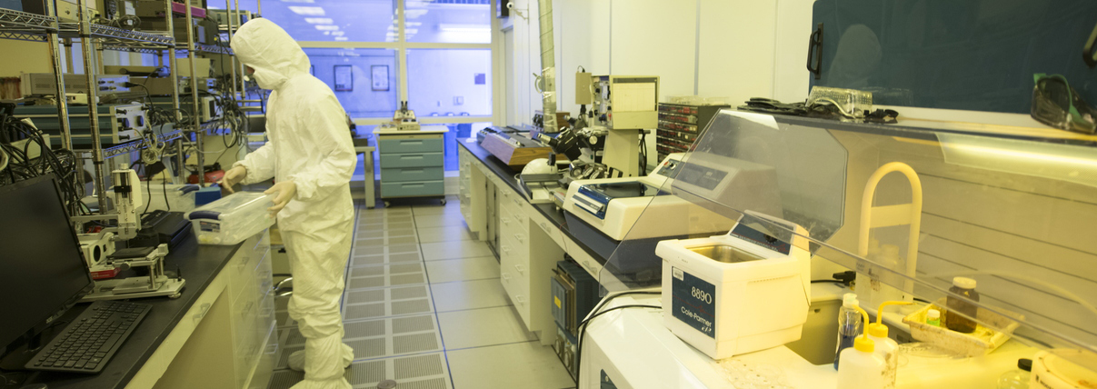
Entry to the MRDL requires clean room protocols. Air flow is from ceiling to floor and is laminar. A clean room environment is maintained by removing airborne particulate larger than 0.5 microns (500 nanometers) in size.

The room is maintained at a constant positive air pressure to minimize outside air contamination. Temperature and humidity are controlled.

Yellow lighting is used for safe processing of light-sensitive materials and chemicals. An ultra-pure deionized water system is used for cleaning.

Lab safety systems and policies are monitored to ensure a safe environment. Please review our lab safety guidelines before using the lab.

Work areas:

  • 2,500 square feet of Class 100 (ISO Class 5) work area
  • 1,750 square feet of Class 1000 (ISO Class 6) work area
  • 950 square feet of Class 10000 (ISO Class 7) work area

Class 100 is defined as fewer than 100 airborne particles larger than 0.5 microns per cubic foot of air. Normal particle count in Class 100 areas is less than 10. In outside air, particle counts can range from 500,000 to several million.

Hybrid Microelectronic Lab (Class 1000 Environment)

Used for thick film screen printing, drying and firing of electrical circuits on ceramic substrates. This is a highly reliable method of electronic circuit fabrication for use in high temperature and robust environments.

Fabrication tools:

  • Integrated circuit die attach
  • Integrated circuit electrical wire bond connectiing
  • Electrical component solder reflow connecting
  • Silicon/ceramic wafer dicing
  • Laser cutting system

Metrology tools:

  • Surface profile measurement of surface roughness and feature thickness
  • Video measurement system for determining width, length and height distances
  • Die shear and wire bond pull testing
Thin Film Lab (Class 100 Environment)

For thin film deposition of multiple materials including conductors, semiconductors and insulators. Materials are accurately deposited in a controlled environment - typically a vacuum chamber with a process gas. The typical thickness is from one to several thousand nanometers.

Thin films are used for electrical device connection, optical components and filters and protective coatings for corrosion and wear. Typical commercial applications include mirrors, sunglasses, cell phone displays, drill bit hardness coatings and solar cells.

Fabrication tools:

  • Resistive evaporation
  • Electron beam evaporation
  • DC magnetron sputtering
  • Ion beam sputtering
  • Pulsed laser deposition

Metrology tools:

  • White light interferometer (measures film surface roughness and film growth)
  • Atomic force microscopy (measures film surface roughness and film growth)
  • Electron diffraction system on pulsed laser deposition system (measures growth of crystalline thin film materials)
  • Ellipsometry (measures thickness of transparent films)
Semiconductor Lab (Class 100 Environment)

For fabrication of electronic devices. Fabrication techniques used in this lab include chemical vapor deposition, reactive ion etching, chemical etching and photolithography. Products include semiconductor devices, integrated circuits, sensors, electrical components and solar cells.

Fabrication tools:

  • Semiconductor process furnace
  • Photolithographic alignment and exposure (single and double sided)
  • Photolithographic chemical dispense and process
  • Reactive ion etching
  • Chemical etching and cleaning

Metrology tools:

  • Transparent thin film measurement system
  • Material electrical impedence measurement
  • Thin film stress gauge
  • Optical microscope
Photomask/Photo Plotter Labs (Class 100 Environment)

For generation of artwork patterns on a photomask (glass plate) or mylar (plastic) sheet for use in photolithographic processing - using light-sensitive chemicals and ultraviolet lights to create patterns on process parts.

A photomask is a very accurate patterned thin metallic coating on glass defined by opaque and transparent areas. The coating material is typically chromium, which blocks ultraviolet light. Feature sizes can range from 1 micron to thousands of microns

A mylar film is a flexible photographic film used to devine patterns containing opaque and transparent regions. Feature sizes can range from 25 microns to thousands of microns.

Fabrication tools:

  • Photomask generation and exposure system
  • Laser photoplotter for mylar film fabrication

Metrology tools:

  • Microscopes for critical optical dimensional measurements
  • Optical microscopes for inspection
Analysis Lab (Class 10000 Environment)

For electronic device and material characterization. In this lab you can test the electrical properties of devices fabricated in the facility and characterize the electrical properties of materials.

Metrology tools:

  • Semiconductor parameter analyzer for current voltage and capacitance voltage measurements
  • Probe stations and light-dark boxes
  • Radio frequency network analyzer
  • Magnetic field test system
  • Cryogenic test systems

Industrial Research and Development

The Microelectronics Research and Development Lab is available for industrial research and development. For information about gaining access to the lab and hourly rates, company representatives should contact Venumadhav Korampally, Ph.D. 

Contact Us

College of Engineering and Engineering Technology
Engineering Building
590 Garden Rd, DeKalb, IL
815-753-2256
ceet@niu.edu
Back to top