Superconducting Films Containing Arrays of Nanoscale Holes
Superconducting films containing periodic hole-arrays have been the subject of much interest in recent years. They provide a unique platform to study generic problems appearing in many physical systems, for example, frustration and interaction between a periodic elastic medium and an array of obstacles. Rich novel vortex phenomena such as the existence of composite vortex lattices, the rectification and phase locking of vortices, commensurate pinning effect, vortex domain formation, and the appearance of multi-quanta vortices have been revealed in this novel system.
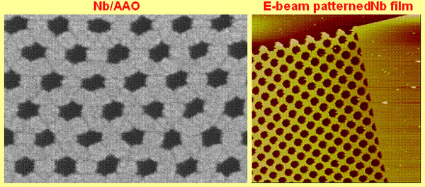
Hole arrays have been usually fabricated by photo- and/or electron beam (e-beam) lithography methods. We developed a new approach to introduce nanoscale hole arrays into superconducting films by utilizing porous substrates arrays [U. Welp et al., Physical Review B 66, 212507 (2002); U. Patel et al. Physical Review B 76, 020508 (R) (2007)]. The porous substrates we have been using are anodic aluminum oxide (AAO) membranes which contain arrays of nanochannels. This approach enabled us to achieve hole diameters as small as a few nanometers and hole spacing down to tens of nanometers. E-beam lithography and focused ion beam (FIB) milling have also being used to pattern superconducting films (Nb, MoGe) and nanoribbons (BSCCO) for this purpose [S. Avci et al., Applied Physics Letters 97, 042511 (2010)].
We carry out both transport and magnetization measurements to study superconducting films containing hole-arrays of various degrees of order of the hole distribution and different ratios between hole diameter and hole spacing. The influence of hole shapes on the physical properties is also being investigated.